I have bought a CNC router to iterate on electronic designs even faster. Here’s what hardware and software I use, and how to mill, drill and cut the board at home.
Table of Contents
What about PCB fabs?
Ordering from JLCPCB or PCBWay is a viable solution, but only if you are 100% sure your design is what you want. Each board will have a soldermask, silkscreen, plated vias and multiple layers. The price is so low that there is no risk of taxes related to the value of the package. PCB fabs can also do SMD assembly, 3D printing and CNC machining.
However, milling at home is better if you simply can’t wait more than a week for delivery of the board, but at the same time, you are unable to test the circuit on the breadboard (small components, too much noise, etc.) Shipping options from China are limited (no delivery to parcel lockers), and usually you have to order at least 5 boards you may find no purpose for.
My workflow
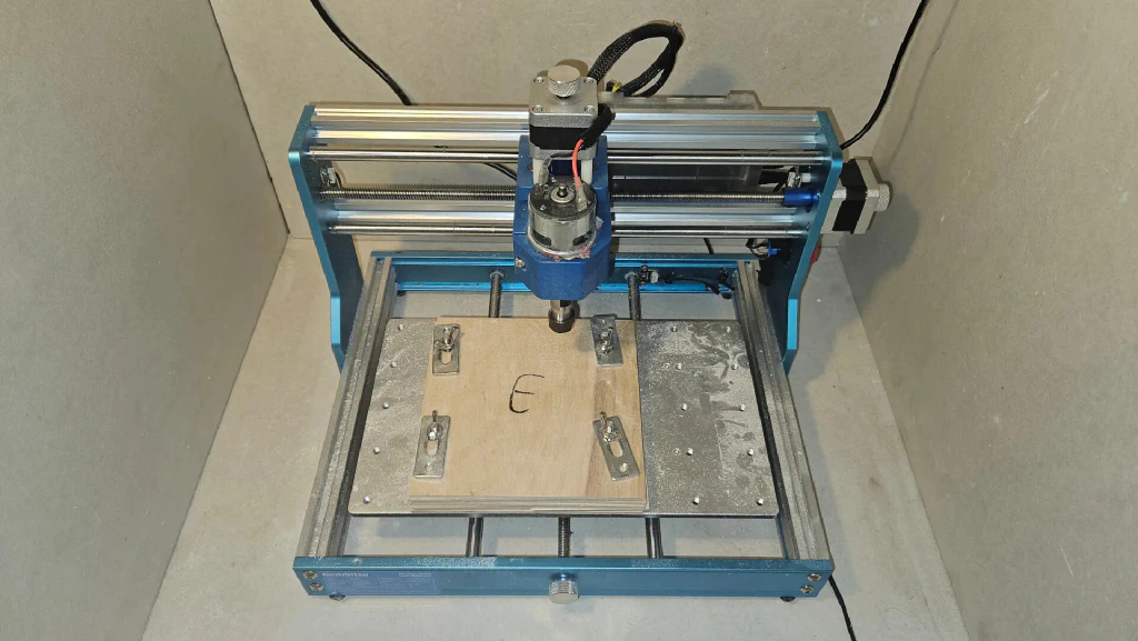
I was looking for a simple, portable CNC device with basic safety features such as a height probe (Z probe) and limit switches. I have found used SainSmart 3018-PROVer V2 online. The router had a scratched spoilboard and the package was incomplete (missing a single clamp and the entire set of V-bits). But hey, the entire thing was inexpensive, and it works fine so far, despite some skill issues on my end.
The downside of the device is the noise it emits. If you set the spindle speed to more than 1000 RPM, the vibrations become so annoying that you have to do some soundproofing – I’ve made a simple enclosure out of a sheet of OSB and some drywall.
I’m also slightly disappointed with the Z axis precision. The Y axis guiderails and the spindle mount do bend a little, and all inaccuracies add up.
KiCad is my PCB design software of choice. It’s open source, and it works on
Linux1 (available on Flathub). It might be annoying to use, but it’s better
than paying for EAGLE Fusion 360 or trying to work around the limitations of
its non-commercial version. It’s easy to create new symbols and footprints in
KiCad, but usually you’ll find them in the built-in library or online. There are
3D models for select components as well. Finally, you can run batch tasks using
the Python scripting console.
People often recommend FlatCAM to postprocess Gerber/Excellon files, and Candle to control the router. These are, in my honest opinion, the worst choices. FlatCAM has an overcomplicated user interface that is changed on every single release, so all video tutorials become useless in no time. Parameter options conflict with each other, and there are no basic optimization features such as milling path reduction or a reasonable drilling order. Candle’s UI does not fit on a smaller screen, auto-leveling seems not to work properly, and you can’t run this app on modern Linux distros even in Xorg mode. I’ve used a Windows virtual machine to work around these issues, but eventually, I switched to pcb2gcode and Universal Gcode Sender (UGS).
Setting up KiCad
Initially, I wasn’t using fine V-bits because I was afraid that they would break or wear down easily, but I was wrong.
I prefer to mill PCBs with a 0.2 mm 45° V-bit (which is effectively 0.4 mm at the Z depth of 0.3 mm), cut the outline with a 1.5 mm bit, and drill holes with a 1 mm drill. I also have 1.5 mm, 2.5 mm and 3.175 mm drills for mounting holes and slots.
You should set up board parameters in the File - Board Setup window right
after you create a new KiCad project. The values listed below are very
conservative (the PCB would look like a heavily customized stripboard), but I
can guarantee they will work with any 3018, no matter how cheaply made.
- Design Rules - Constraints
- Minimum clearance: 0.5 mm
- Minimum track width: 0.5 mm
- Copper to hole distance: 0 mm
- Copper to edge distance: 0 mm
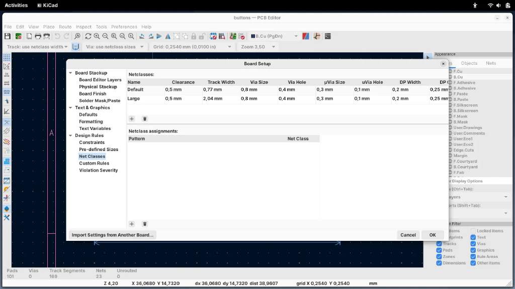
- Design Rules - Net Classes
- “Default”
- Clearance: 0.5 mm
- Track width: 0.77 mm
- “Large” (add new)
- Clearance: 0.5 mm
- Track width: 2.04 mm
- “Default”
Observe that 0.77 + 0.5 = 1.27 and 2.04 + 0.5 = 2.54. Common pin headers have 0.1 inch (2.54 mm) spacing. The values I’ve picked make routing easier, but having parallel routes close to each other may be a bad idea for analog signals.
Once you get comfortable using the router, you can try smaller components. I’ve successfully cut the breakout board for both TQFP32 chip (0.8 mm pitch) and SSD1306 display (0.65 mm pitch). I believe that, with enough patience, USB‑C receptacle (commonly 0.5 mm) is also doable.
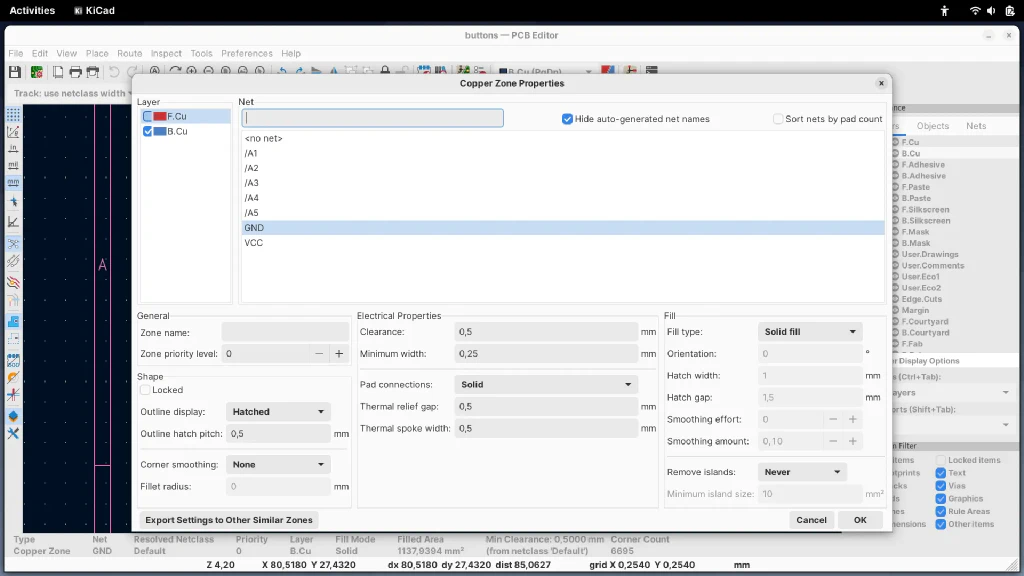
It’s a good practice to set the empty area between traces as a ground zone. It’s challenging because there is only one layer, the bottom one. However, you can draw on the top layer and use jumper wires on a real board. Make sure islands (unconnected ground planes) are not removed.
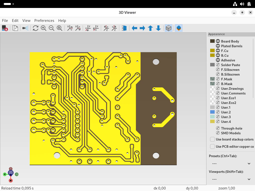
Finally, it may be useful to enlarge pads to make the soldering easier. It is possible to change their shape as well. The maximum reasonable area for the parameters listed above is 2.04 mm × 2.04 mm. Rectangular pads are difficult to work with due to the lack of a soldermask, so I would recommend having these oval or circular. Pads can be modified manually, but you can also use the scripting console (KiPython). This is an experimental feature, so you should remember to save your changes before running any code, or you will lose progress when KiCad crashes.
To modify the pads, copy the following code, open KiCad console, and paste with Ctrl+Shift+V.
import pcbnew

board = pcbnew.GetBoard()

mm = pcbnew.PCB_IU_PER_MM
pad_min = int(2.04 * mm)
drill_min = int(1 * mm)

for p in board.GetPads():
    # Ignore holes:
    if not p.GetNetname():
        continue
    # Ignore surface mount pads:
    pad_w, pad_h = p.GetSize()
    drill_w, drill_h = p.GetDrillSize()
    if drill_w == 0 and drill_h == 0:
        continue
    # Enlarge THT pads and holes:
    p.SetSize(pcbnew.VECTOR2I(max(pad_min, pad_w), max(pad_min, pad_h)))
    p.SetDrillSize(pcbnew.VECTOR2I(max(drill_min, drill_w), max(drill_min, drill_h)))
    p.SetShape(pcbnew.PAD_SHAPE_OVAL)

pcbnew.Refresh()
The final result looks really promising:
Exporting Gerber files
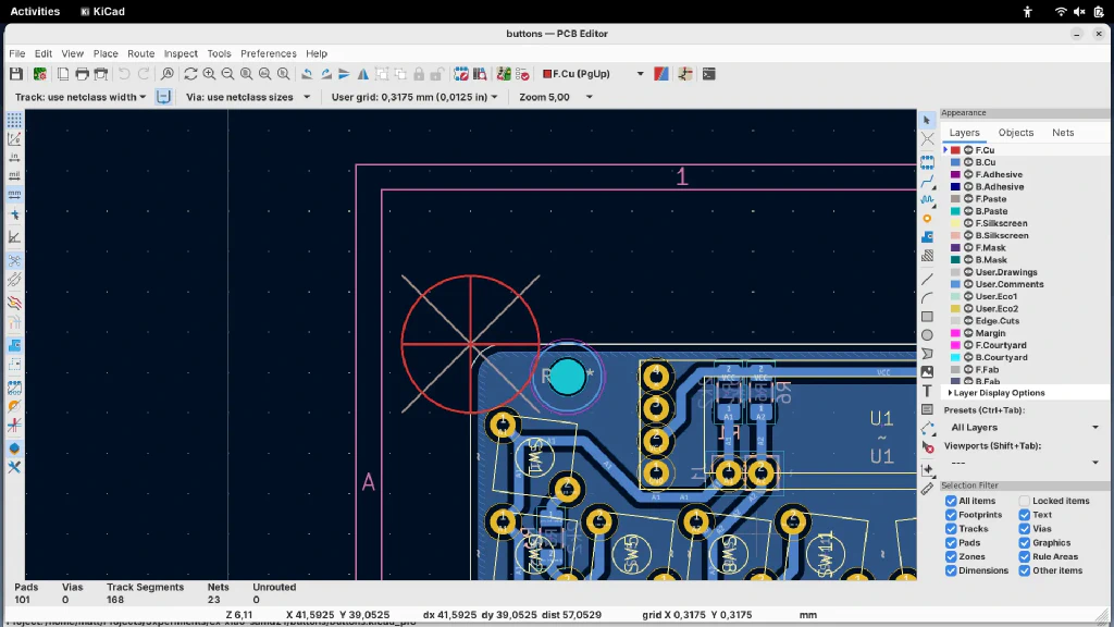
The default (0, 0) point is in the top-left corner of the PCB drawing sheet, but
it has to be moved to the top-left corner of the actual PCB to make spindle
moves predictable. Use menu options Place > Drill/Place File Origin and
Place > Grid Origin to match the picture below.
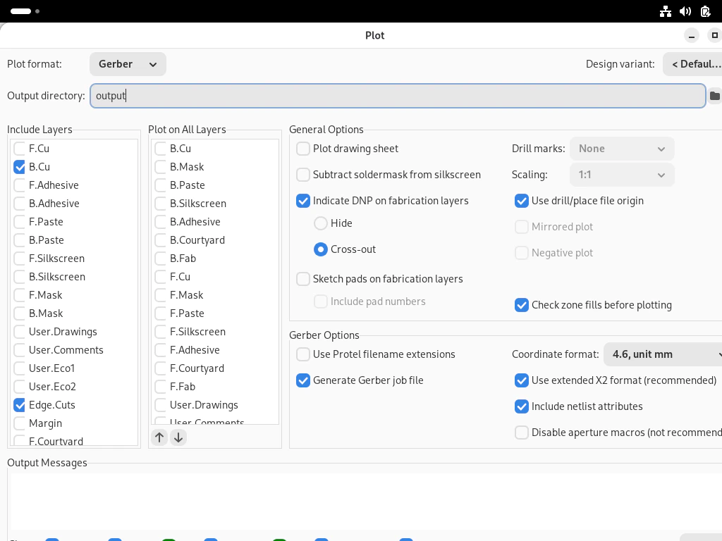
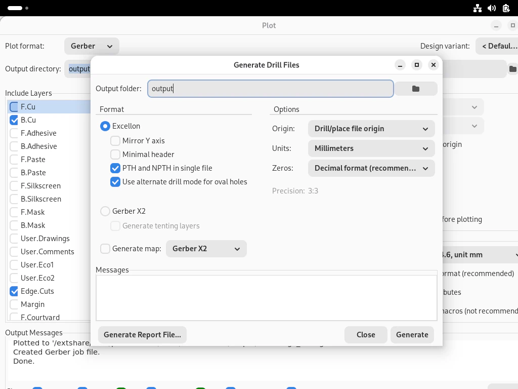
Gerber files for milling (B.Cu and Edge.Cuts layers) and cutting, and Excellon
files for drilling, can all be exported from the File > Plot menu. Create all
new files in a separate output directory. Make sure the following options are
enabled:
Use drill/place file originUse alternate drill modePTH and NPTH in a single file
Converting to G-code
I’ve already mentioned that I use pcb2gcode for converting KiCad output files
to G-code. It’s a command line program, which is a blessing and a curse. You can
(or have to) update a single millproject file to adjust the parameters.
There are no prebuilt executables, but here comes Docker to the rescue.
Create Dockerfile next to the original PCB files and paste this:
FROM debian:13

RUN apt-get update \
    && apt-get install git cmake build-essential pkg-config libboost-program-options-dev libboost-test-dev libgtkmm-2.4-dev gerbv librsvg2-dev -y \
    && sed -i 's/Version:/Version: 2.10/g' /usr/lib/x86_64-linux-gnu/pkgconfig/libgerbv.pc

RUN git clone https://github.com/pcb2gcode/pcb2gcode.git \
    && cd pcb2gcode \
    && git checkout v3.0.4 \
    && cmake -S . -B build -DPCB2GCODE_COMPILE_WARNING_AS_ERROR=OFF \
    && cmake --build build -j$(nproc) \
    && cp /pcb2gcode/build/pcb2gcode /usr/bin/

RUN useradd -u 1000 user
USER user

WORKDIR /output
ENTRYPOINT bash -c "pcb2gcode && rm *.svg"
Create another file, compose.yml, and paste this YAML there:
services:
  main:
    build: .
    image: pcb2gcode:3.0.4
    volumes:
      - ./output:/output
At last, enter the output directory (the one with Gerber files) and create
millproject file:
# general

metric = true
metricoutput = true
nog64 = true
nom6 = true
zchange = 2.0mm
zsafe = 2.0mm

back = [project name]-B_Cu.gbr
back-output = [project name]-B_Cu.gbr.ngc
drill = [project name].drl
drill-output = [project name].drl.ngc
outline = [project name]-Edge_Cuts.gbr
outline-output = [project name]-Edge_Cuts.gbr.ngc

# milling

mill-diameters = 0.4mm
mill-feed = 200mm/min
mill-infeed = 0.15mm
mill-speed = 1500rpm
voronoi = true
zwork = -0.3mm

# drilling

drill-feed = 50mm/min
drill-side = back
drill-speed = 1500rpm
drills-available = 1.0mm, 2.5mm
nog81 = true
zdrill = -[board thickness + 0.4]mm

# cutting

cut-feed = 100mm/min
cut-infeed = 0.15mm
cut-side = back
cut-speed = 1500rpm
cutter-diameter = 1.5mm
zcut = -[board thickness + 0.2]mm
bridges = 1.0mm
bridgesnum = 4
zbridges = -[zcut - 1.0]mm
Now you can run the pcb2gcode with simple docker compose up.
Some lines in the configuration file need a short explanation:
- The output is mirrored, because copper is present only on the back of the board.
- Traces are converted into Voronoi areas, greatly reducing the total length of milling.
- Drilling and cutting depths are larger than actual thickness of the material on purpose.
- Some thin bridges are added when cutting outline, otherwise the board could “fly” away.
- The router’s firmware (GRBL) seems not to support some G-code instructions.
If you’ve used 3D printer before, some concepts may sound familiar (for example cutting in multiple passes is similar to having multiple layers on 3D prints). In both cases, the G-code is used to control the machine.
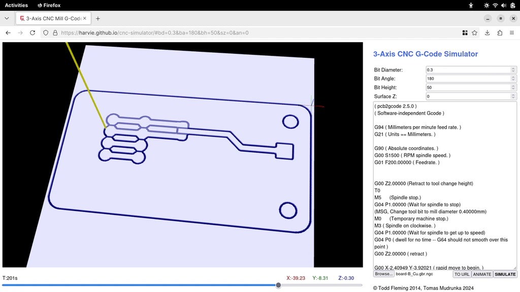
You can inspect .ngc files using G-code utilities that run in your browser. Previously I’ve used NCViewer, but I found a more advanced program that can actually show the cut diameter and rotate objects in 3D space.
Milling the PCB
WARNING: I take no responsibility for any damage to your health or property.
It’s time to finally turn the copper-clad laminate into a useful circuit board. Secure it onto the spoilboard and make sure that the spindle would be able to move freely in the Z axis. Use double-sided tape for larger or thinner boards if necessary. Insert the milling bit and then attach the Z probe (you may have to modify it and add the second alligator clip).
Open the Universal Gcode Sender (UGS), connect to the router, and move the
spindle to the top-right corner of the usable area. Lower the spindle until the
probe’s LED turns red. Click Reset Zero and then Return to Zero to make sure
the router is calibrated.
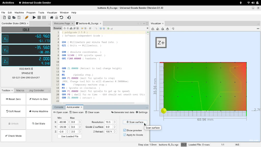
Auto-leveling: Load the bottom layer file and open the AutoLeveler plugin
(Window > Plugins > AutoLeveler). Click Use loaded file to resize the height
map. Change the Z axis range to -2 mm to 2 mm. The resolution of about
10 mm should be fine. Start the AutoLeveler and wait for the scanning to be
completed. Save the height map for later, it will be useful if UGS crashes.
Disconnect the height probe and click Return to Zero. Do not run
AutoLeveler again once you have milled the board, it will not work as expected
because copper areas are not connected anymore.
Milling: Make sure bottom layer file is loaded and the AutoLeveler’s
Apply to Gcode option is checked. Click Send (the “play” button). The
spindle will move up a little. Click Send again to actually start the milling.
Return to Zero once the job is done. Inspect the board; it may be necessary to
run the process again if some tracks look incomplete.
Cutting: Press the emergency button, raise the spindle, insert a new bit, lower the spindle to make it barely touch the board, then release (rotate) the button. Open the outline file and repeat the steps above.
Drilling: Repeat the steps above. If you have specified multiple drill
diameters in millproject file, the machine will temporarily stop when it’s
time to change a tool - press Start when you’re ready to continue.
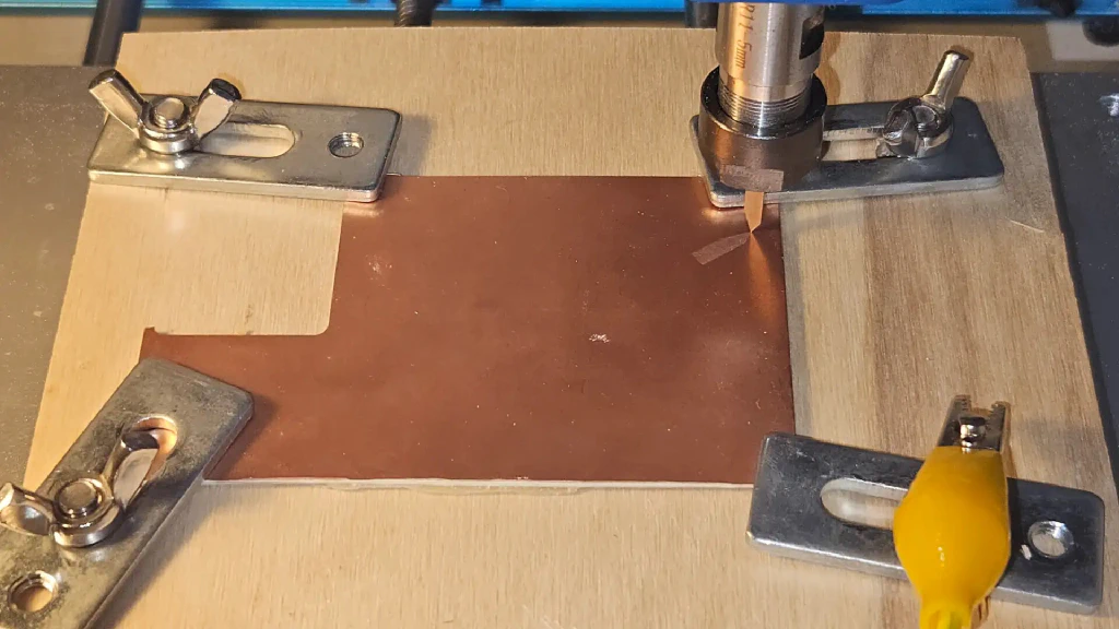
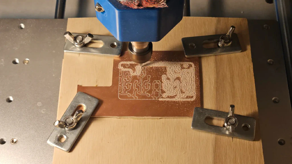
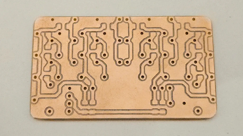
At last, detach the PCB from the spoilboard. Use some coarse sandpaper to finish the edges of the PCB if necessary, expand the mounting holes using a power drill, and install all electronic components according to the schematic. Use extra flux to make soldering easier.
Soldermask
There are two methods of applying a UV-curable soldermask to the PCB. First, you can add a few drops of such resin onto the finished board, use a thin film and a sharpie pen to mask solder points, expose the resin, and then remove the remaining resin with isopropyl alcohol. This may be the more annoying option because you have to guess how long the board has to be exposed, and the uncured soldermask will get stuck in drilled holes.
Another approach is to drip some resin onto the board right after milling, then remove it mechanically. This option has some disadvantages when paired with my CNC router. The copper layer is really thin, and you will either damage PCB traces or skip some solder points. A 10×10 cm board is far too large. It may work fine for smaller PCBs, though.
I think that it’s not worth it. I’ve spent a lot of time and money trying, and it didn’t work well. If you really need a soldermask, then mill a prototype, test it, and then order PCBs online. Remember that a soldermask is not an insulation layer, and it is only used to make soldering easier and to protect the copper from oxidation.
Random tips and tricks
Start with some smaller designs if this is your first time milling PCBs. Make sure to understand basic concepts, such as homing the device. If you consider yourself more experienced, remember that mistakes may happen anyway.
Be aware that your CNC router is a relatively cheap device, and it may be counterintuitive in use. Try out various feed rates and spindle speeds and find the best values for reduced noise and vibrations and prolonged device life. My CNC router’s spindle can reach crazy fast speeds, but in practice, 1500 RPM is good enough.
Try out multiple base materials and understand the difference between them. I prefer the 1.6 mm phenolic paper laminate, which I believe is also known as FR1/FR2. It’s super easy to cut due to its soft structure similar to the prototyping perfboard. Another good candidate is a 1.0 mm FR4 board, which should be more durable but is harder to work with.
Learn the basics of G-code. It’s possible to move the spindle manually with a
knob, but the router will not know about this change. If you run G-code
commands, then the internal device state is updated, and UGS actions such as
Return to Zero can work properly. You should know how G0, G90/G91 and
M3/M4/M5 can be used, and how to modify .ngc files to skip commands. I have
found good G-code documentation online to
help you get started.
Your CNC router can do more than printed circuit boards. Use it to cut plastic, wood and (softer) metals. I’ve tried making electronic enclosures out of acrylic (thin 0.85 mm plexiglass from the clip frame) and got acceptable results. Of course, you need to adjust the spindle rotation speed and feed rate accordingly. The softening point of PMMA is only 90°C, so the removed material will melt around the cutting bit if you’re not super careful.
-
It works, but there are huge performance issues on Wayland if there is at least one maximized KiCad window. You need to open the
dconf-editor, setorg.gnome.mutter.auto-maximizetofalse, and then manually resize KiCad windows to the maximum possible size. KiCad is also difficult to work with if you have fractional scaling enabled. ↩︎